How to Use an MMC
Apr 17, 2006
Now SD Memory Card (Secure Digital Memory Card) is the most popular
memory card for mobile equipments. The SD Memory Card (SDC below) was developped
as upper-compatible to Multi Media Card (MMC below) so that the SDC
compleant equipments can also use an MMC with a few considerations. There are
also reduced size versions, such as RS-MMC, miniSD and
microSD, with same function. The MMC/SDC has a microcontroller in it,
the flash memory controls (erase, read, write and error control) are completed
at inside of the memory card. The data is transferred between memory card and
host controller in unit of 512 bytes per block in default, so that it can be
seen like a generic hard disk drive from view point of application programs. The
currentry defined file system is only FAT12/16 with FDISK patitioning rule. The
FAT32 is defined for only high capacity (>= 2G) cards.
This page describes the basic knowledge and miscellaneous things that I
become aware, on using MMC/SDC with small embedded system. I believe that this
information will be a useful technical note for people who is going to begin to
enjoy MMC/SDC.
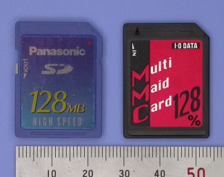
Contact Surface
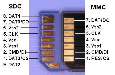
Right photo shows the contact surface of the SDC/MMC. The MMC has seven
contact pads and the SDC has nine contact pads that two pads added to MMC. Three
of the contacts for each occupy as power supply pins so that the effective
signal numbers are four and six. Ofcourse the data transfer betwenn the host and
the card is done in clocked serial data transfer.
The working supply voltage range is indicated in OCR register and it should
be read to comfirm the operating voltage range. However, the supply voltage can
be fixed to a proper value because the MMC/SDC works at supply voltage of
2.7 to 3.6 volts at least. The current consumption can reach up to
several ten milliamperes at worst case, the host system should able to supply
100 miliamperes.
SPI Mode
SPI mode is an alternative
operating mode that defined to use MMC/SDC without its specific host interface.
The communication protocol for the SPI mode is very simple compared to MMC/SDC
native mode, the MMC/SDC can be attached via a generic SPI port or a GPIO port
built in most microcontrollers. Therefore the SPI mode is suitable for low cost
embedded applications. Especialy, there is no reason to use native mode for
electronic handiwork as a hobby. For SDC, the 'SPI mode 0' is defined for
its SPI mode. But for MMC, it is not the SPI timing, both latch and shift
actions are defined with rising edge of SCLK, but it seems work in SPI mode 0 at
SPI mode. Thus SPI Mode 0 (positive clock, front edge latch, back edge
shift) is the proper setting for MMC/SDC interface, and SPI mode 3 also works as
well.
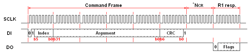
Command and Response
In SPI mode, the data direction on the signal line is fixed and the data is
transferred in byte oriented serial communication. The command frame from host
to card is a fixed length (six bytes) packet that shown below. When a command
frame is transmitted to the card, a response to the command (R1, R2 or R3) will
be sent back to the host. Because data transfer is driven by serial clock
generated by host, the host must continue to read bytes until receive an
effective response. The command response time (NCR) is 0 to 8
bytes for SDC, 1 to 8 bytes for MMC. The CS signal must be held low during a
transaction (command, response and data transfer if exist). The CRC field is
optional in SPI mode, but it is required as a bit field to compose a command
frame.
SPI Command Set
Each command is expressed in abbreviation like GO_IDLE_STATE or CMD<n>,
<n> is the number of the command index and the value can be 0 to 63.
Following table describes only commands that to be usually used for generic
read/write and card initialization. For details on all commands, please refer to
spec sheets from MMCA and SDCA.
Command
Index |
Argument |
Response |
Data |
Abbreviation |
Description |
| CMD0 |
None(0) |
R1 |
No |
GO_IDLE_STATE |
Software reset. |
| CMD1 |
None(0) |
R1 |
No |
SEND_OP_COND |
Initiate initialization process. |
| ACMD41(*1) |
None(0) |
R1 |
No |
APP_SEND_OP_COND |
For only SDC. Initiate initialization process. |
| CMD9 |
None(0) |
R1 |
Yes |
SEND_CSD |
Read CSD register. |
| CMD10 |
None(0) |
R1 |
Yes |
SEND_CID |
Read CID register. |
| CMD12 |
None(0) |
R1b |
No |
STOP_TRANSMISSION |
Stop to read data. |
| CMD16 |
Block
length[31:0] |
R1 |
No |
SET_BLOCKLEN |
Change R/W block size. |
| CMD17 |
Address[31:0] |
R1 |
Yes |
READ_SINGLE_BLOCK |
Read a block. |
| CMD18 |
Address[31:0] |
R1 |
Yes |
READ_MULTIPLE_BLOCK |
Read multiple blocks. |
| CMD23 |
Number of
blocks[15:0] |
R1 |
No |
SET_BLOCK_COUNT |
For only MMC. Define number of blocks to transfer
with next
multi-block read/write command. |
| ACMD23(*1) |
Number of
blocks[22:0] |
R1 |
No |
SET_WR_BLOCK_ERASE_COUNT |
For only SDC. Define number of blocks to pre-erase
with next
multi-block write command. |
| CMD24 |
Address[31:0] |
R1 |
Yes |
WRITE_BLOCK |
Write a block. |
| CMD25 |
Address[31:0] |
R1 |
Yes |
WRITE_MULTIPLE_BLOCK |
Write multiple blocks. |
| CMD55(*1) |
None(0) |
R1 |
No |
APP_CMD |
Application specific command. |
| CMD58 |
None(0) |
R3 |
No |
READ_OCR |
Read OCR. |
| *1:ACMD<n> means a command sequense of
CMD55-CMD<n>. |
SPI Response
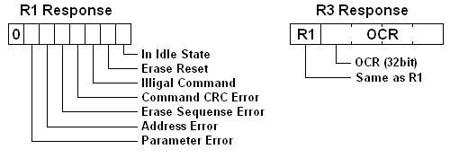
There are three command response formats, R1, R2 and
R3, depends on each command. A byte of response R1 is returned for most
commands. The bit field for R1 response is shown in right image, and a 0x00 zero
means successful. When any error occured, corresponding bit will be set. The R3
response is for only CMD58, its first byte is same as R1 and is trailing the
content of OCR.
Some command takes a time longer than NCR and it responds
R1b that is R1 response followed by busy flag (DO is held low as long
as internal process is being executed). The host controller shuld wait for end
of the process until 0xFF is received.
Initialization Procedure for SPI Mode
After power on reset, MMC/SDC enters its native operating mode. To put it SPI
mode, follwing procedure must be performed.
Power ON (Insersion)
After supply voltage reached 2.2 volts, wait for a millisecond at least,
set DI and CS high and apply more than 74 pulses to SCLK and the card
will able to accept a native command.
Software Reset
Send a CMD0 with CS low to reset the card. The card samples CS
signal when a CMD0 is detected. If the CS signal is low, the card enters SPI
mode. Since the CMD0 must be sent as a native command, the CRC field must have a
valid value. When once the card enters SPI mode, the CRC check is disabled and
the CRC value is negligible, so that command transmission routine can be written
with the hardcorded CRC byte of 0x95 that valid for only CMD0. When the CMD0 is
accepted successfuly, the card will enter idle state and respond R1 response
with In Idle State bit (0x01). The CRC can also be re-enabled with CMD59.
Initialization
In idle state, the card accept only CMD0, CMD1 and CMD58. Any other commands
will be rejected. When the card detects a CMD1, it starts
initialization. To poll end of the initialization, host controller must repeat
to send CMD1 and check the response. When the card is initialized successfuly,
In Idle State in the R1 response is cleared (0x00). The initialization process
can take several hundred milliseconds (large cards tend to longer), so
that this is a consideration to determin the time out value. After the
initialization has finished, generic read/write will be accepted. In this time,
OCR and CID may be read to confirm operating voltage range, card size or any
properties if needed.
For SDCs, ACMD41 instead of CMD1 is recommended to initiate
initialization. The CMD1 seems to not work on some SDCs, so that a retry
sequense with ACMD41 should be done when CMD1 is rejected or a time out is
occured during idle polling.
Data Transfer
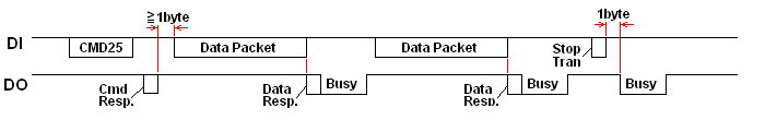
Data Packet and Data Response
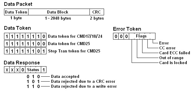
In a transaction with data transfer, one or more data blocks will be
sent/received after command response. The data block is transferred as a data
packet that consist of Token, Data Block and CRC. The format of the data packet
is showin in right image and there are three data tokens. As for Stop Tran token
that means end of multiple block write, it is used in single byte without data
block and CRC.
Single Block Read
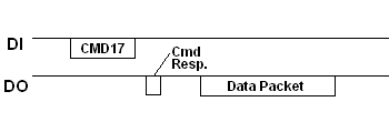
The argument specifies the location to start to read in unit of
byte. The sector address specified by upper layer must be scaled to byte
address. When a CMD17 is accepted, a read operation is initiated and the read
data block will be sent to the host. After a valid data token is detected, the
host controller receives following data block, and two byte CRC must be flushed
even if it is not needed. The block size is 512 bytes in default and it can also
be changed with a CMD16. If any error occured during read operation, an error
token will be returned instead of data packet.
Multiple Block Read
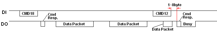
The Multiple Block Read command reads multiple blocks in sequense from the
specified address. When number of transfer blocks has not been sepecified before
this command, the transaction will be initiated as an open-ended multiple block
read, the read operation will continue until stopped with a CMD12. The received
byte immediataly following CMD12 is a stuff byte, it should be discarded before
receive a response of the CMD12.
Single Block Write
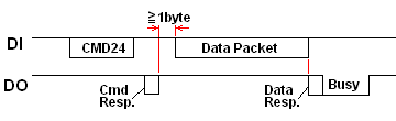
When a write command is accepted, the host controller sends a data packet to
the card after a byte space. The packet format is same as Block Read command.
When a data packet has been sent, the card responds a Data Response immediataly
following the data packet. The data response trails a busy flag to process the
write operation. Most cards cannot change write block size and it is fixed to
512.
In principle of the SPI mode, the CS signal must be asserted during a
transaction, however there is an exception to this rule. When the card is busy,
the host controller can deassert CS to release SPI bus for any other SPI
devices. The card will drive DO signal low again when reselect it during
internal process is in progress. Therefore a preceding busy check (wait ready
immediataly before command and data packet) instead of post wait can eliminate
waste wait time. In addition the internal process is initiated a byte after the
data response, this means eight clocks are required to initiate internal write
operation. The state of CS signal during the eight clocks is negligible so that
it can done by bus release process described below.
Multiple Block Write
The Multiple Block Read command writes multiple blocks in sequense from the
specified address. When number of transfer blocks has not been sepecified before
this command, the transaction will be initiated as an open-ended multiple block
write, the write operation will continue until terminated with a Stop Tran
token. The busy flag will appear a byte after the Stop Tran token. As for SDC,
the multiple block write transaction must be terminated with a Stop Tran token
independent of pre-defined or open-ended.
Reading CSD and CID
These are same as Single Block Read except for the data block length. The CSD
and CID are sent to the host as 16 byte data blocks. For details of the
CMD, CID and OCR, please refer to the MMC/SDC specs.
Cosideration to Bus Floating and Hot Insertion
Any signal that can float should be pulled low or high properly via a
resister. This is a generic design rule on MOS devices. Because DI and DO are
normally high, so that they should be pulled-up. According to SDC/MMC specs,
from 50k to 100k ohms is recommended to the value of pull-up registers. However
the clock signal is not mentioned in the SDC/MMC specs because it is usually
driven by host controller. When there is a time that it can float, it should be
pulled to the normal level, low.
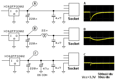
The MMC/SDC can hot insertion/removal but some consideration to the host
circuit are needed to avoid an incorrect operation. For example, if the system
power supply (Vcc) is tied to the card socket directly, the supply voltage will
dip at the instant of contact closed due to charge current to the capacitor that
built in the card. 'A' in the right image is the scope view and it shows that
occureing a voltage dip of 600 millivolts. This is a sufficient level to trigger
brown out detector. 'B' in the right image shows that an inductor is inserted to
block pulse current, the voltage dip is improved to 200 millivoits. A large
OS-CON can improve the voltage dip dratiscally. However the OS-CON can cause an
oscillation of LDO regulator.
Cosideration on Multi-slave Configuration
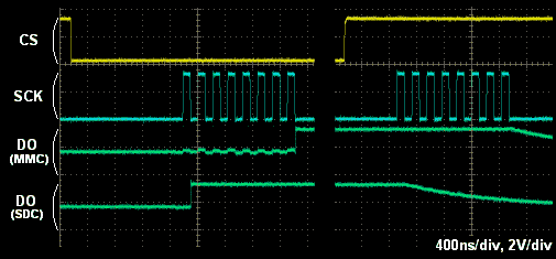
In SPI, each slave device is selected with separated CS signals, and plural
devices can be attached to an SPI bus. Generic SPI slave device drives/releases
its DO signal by CS signal asynchronously to share an SPI bus. However MMC/SDC
drives/releases DO signal in synchronising to SCLK. There is a posibility of bus
conflict when attach MMC/SDC and any other SPI slaves to an SPI bus. Right image
shows the drive/release timing of MMC/SDC (DO is pulled to 1/2 vcc to see the
bus state). Therefore to make MMC/SDC release DO signal, the master device must
send a byte after deasserted CS signal.
Optimization of Write Performance
Most MMC/SDC employs NAND Flash
Memory as a memory array. The NAND flash memory is cost effective and it can
read/write large data fast, but on the other hand, there is a
disadvantage that rewriting a part of data is inefficient. Generally
the flash memory requires to erase existing data before write a new data, and
minimum unit of erase operation (called erase block) is larger than write block
size. The typical NAND flash memory has a block size of 512/16K bytes for
write/erase operation, and recent monster card employs large block chip
(2K/128K). This means that rewriting entire data in the erase block is done in
the card even if write only a sector (512 bytes).
Benchmark
I examined the read/write performance of some MMC/SDC with a cheap 8
bit MCU (ATmega64 @9.2MHz) on the assumption that an embedded system with
limited memory size. For reason of memory size, write() and
read() ware performed in 2048 bytes at a time. The result is: Write:
77kB/sec, Read: 328kB/sec on the 128MB SDC, Write: 28kB/sec,
Read: 234kB/sec on the 512MB
SDC and Write: 182kB/sec, Read: 312kB/sec on the 128MB MMC.
Therefor the write performance of the 512MB SDC was very poor that one third
value of 128MB SDC. Generally the read/write performance of the mass storage
device increases proportional to its recording density, however it sometimes
appears a tendency of opposite on the memory card. As for the MMC, it seems to
be several times faster than SDC, it is not bad performance. After that time, I
examined some SDCs supplied from different makers, and I found that PQI's SDC
was as fast as Hitachi's MMC but Panasonic's and Toshiba's one was very poor
performances.
Erase Block Size
To analys detail of write operation, busy time (number of polling cycles)
after sent a write data is typed out to console in the low level disk write
function. Multiple numbers on a line indicates data blocks and a Stop Tran token
that issued by a multiple block write transaction.
In resulut of the analysis, there is a different of internal process between
128MB SDC and 512MB SDC. The 128MB SDC rewrites erase block at end of the
mutiple block write transaction. The 512MB SDC seems have 4K bytes data buffer
and it rewrites erase block every 4K bytes boundary. Therefor it cannot compared
directly but the processing time of rewriting an erase block can be read 3800
for 128MB SDC and the 512MB SDC taeks 30000 that 8 times longer than 128MB SDC.
Judging from this resulut, it seems the 128MB SDC uses a small block chip and
the 512MB SDC uses a large block or MLC chip. Ofcourse the larger block size
decreases the performance on pertial block rewriting. In 512MB SDC, only an area
that 512K bytes from top of the memory is relatively fast. This can be read from
write time in close(). It might any special processing is applied to
this area for fast FAT accsess.
Improving Write Performance
To avoid this bottleneck and rise write performance of SDC/MMC, writing large
number of blocsks as possible (aligned to erase block is ideal) at a time will
do. In other words, allocate large buffer memory and pass it to
fwrite() will do. For low level disk write function, it must pre-inform
number of write sectors to the card for efficient write processing. This called
`pre-defined multiple block write'. However the pre-definition command is not
the same between MMC (CMD23) and SDC (ACMD23).
Well, it might a vain efforts that to rise write performance of SDC on the
cheap MCUs that have only several kilobytes of RAM. CompactFlash have a good
performance that ten times faster than SDC. When you require a write performance
to the memory card, a CompactFlash or an MMC will be suitable better than
SDC.
The memory cards are initially patitioned and formatted to align the
allocation unit to the erase block. When re-patition or re-format the memory
card with a system that is not compliant to MMC/SDC (this is just a PC) with no
care, the optimization will be broken and the write performance might be lost. I
tried to re-format 512MB SDC in FAT32 with a PC, the write performance measured
in file copy was lowerd to one several. Therefore the re-formatting the card
should be done with MMC/SDC compliant equipments rather than PC.
